- Services
-
Materials Testing and Failure Analysis
- Macroscopy and Stereoscopy
- Metallography / Materialography
- Hardness Testing
- Scanning Electron Microscopy
- Zeiss Merlin Gemini Scanning Electron Microscope
- Chemical and Physical Materials Analyses
- Non-destructive Testing
- X-Ray Inspection Systems
- Environmental Simulation
- Additive Manufacturing
- Powder characterization procedure PowderGenetics®
- Residual Stress Analysis
-
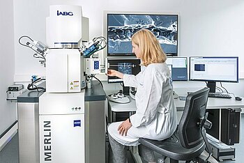
Zeiss Merlin Gemini Scanning Electron Microscope
Zeiss Merlin Gemini Scanning Electron Microscope
The high-resolution field emission scanning electron microscope and an energy dispersive X-ray microarea analysis (EDX) are used to run topography and morphology tests.
A field emitter gives magnifications of up to 500.000 : 1, which corresponds to a resolution of 0.6 nanometres on a sample surface. In addition, very low acceleration voltages can be selected, which permits testing of non-conductive materials like biological samples, plastics or ceramics.
Using four detectors, tests and analyses are performed at acceleration voltages of 0.1 kV to 30 kV in secondary and backscattered electron contrasts.
Application range
- Fractography
- Particle analyses
- Topography examinations
- Qualitative and semi-quantitative determination of materials (EDX)
- Tests on grinding probes
- Asbestos examinations
The tests are provided on a cross-sector and cross-material basis for semi-finished products, samples, components, and metallic and organic materials.
![[Translate to English:] Makroskopie und Stereoskopie](/fileadmin/_processed_/e/6/csm_Makro-Stereoskopie_400x200_95153c2a31.jpg)
![[Translate to English:] Rasterelektronenmikroskop Zeiss Merlin Gemini](/fileadmin/_processed_/5/f/csm_Rasterelektronenmikro_Zeiss_400x200_76ab1dd2d3.jpg)
![[Translate to English:] Umweltsimulation & Schadensanalyse](/fileadmin/_processed_/2/5/csm_Umweltsimulation-Schadensanalyse_400x200_43cde76a55.jpg)
![[Translate to English:] Metallografie / Materialografie](/fileadmin/_processed_/c/9/csm_Meallografie-Materialografie_400x200_8cc43a1051.jpg)
![[Translate to English:] Chemische und physikalische Werkstoffanalysen](/fileadmin/_processed_/a/b/csm_Werkstoffanalyse_400x200_09062cf421.jpg)
![[Translate to English:] Additive Fertigung](/fileadmin/_processed_/5/1/csm_Additive-Fertigung_400x200_44855c2ef5.jpg)
![[Translate to English:] Härteprüfung](/fileadmin/_processed_/9/4/csm_Haertepruefung_400x200_73a4c4559b.jpg)
![[Translate to English:] Zerstörungsfreie Prüfverfahren](/fileadmin/_processed_/6/1/csm_Zerstoerungsf_Pruefverfahren_400x200_aafe80351c.jpg)
![[Translate to English:] Pulvercharakterisierungsverfahren PowderGenetics®](/fileadmin/_processed_/c/d/csm_PowderGenetics_400x200_ab495fe74c.jpg)
![[Translate to English:] Rasterelektronenmikroskopie (REM)](/fileadmin/_processed_/f/7/csm_REM_400x200_f58e0f4e54.jpg)
![[Translate to English:] Röntgeninspektionssysteme](/fileadmin/_processed_/d/3/csm_Roentgeninspektionssystem_400x200_b3d223c6a9.jpg)
![[Translate to English:] Eigenspannungsmessung](/fileadmin/_processed_/e/b/csm_Eigenspannungsmessung_400x200_0c75787702.jpg)